
The Individual assignement of this week was to redraw a echo hello-world board and to add atleast a button and a LED. Further check the design rules, make it and test it stimulating its operations.
For designing the echo hello-world board, I have used Kicad software. The software gives the user a very interactive software. The steps involved in designing an echo hello-world board are as under:-
1. Draw the schematic of the circuit board in Kicad by selecting appropriate components.
2. Further the annotation of the circuit has to be done.
3. Check the electrical design rules.
4. Further proceed for creating a PCB foot print.
The images of the work done during the PCB schematic design is as under:-
Adding components-
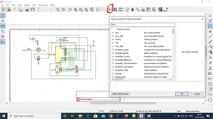
The components can be selected using the highlighted icon. For selecting the right component, the kicad library must be updated. It can be done though https://gitlab.fabcloud.org/pub/libraries/electronics/tree/master/kicad .
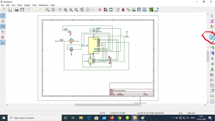
The next step is to connect the components using dag wire tool:-
Further, the foot prints has to be assigned to the schematic. The items checked in the right hand panel of the below image is only required to design PCB.
The design is then annotated using the tool for that as shown in the picture below. The annotation should be complete without error to process further:-
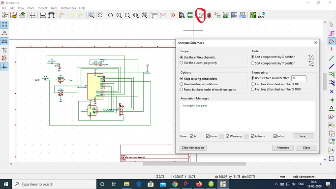
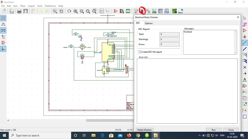
After the completion of the annotation without errors, Electrical check rules are to be executed as shown in the picture below. There were many basic errors in the electrical check rules which were corrected until no errors are left in the design.
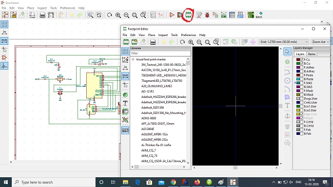
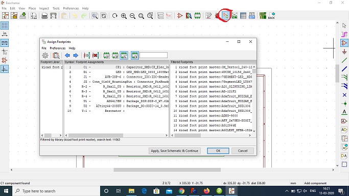
After the electrcial connections are perfect in the design, foot prints are assigned to the PCB. During this process there are many components available in the KICAD library. The user can select the ones available in their labs or somewhat identical components for ease of working. The process executed is shown in the image below:-
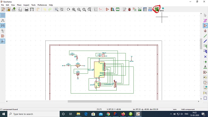
After assigning the footprints to the design, the design is now ready to be converted into the PCB using tjhe tool highlighted in the image below:-
After completion of the above step, a screen would be appearing as under. The schematic designed can be converted into a PCB by the tool update PCB as shown in the image below:-

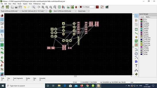
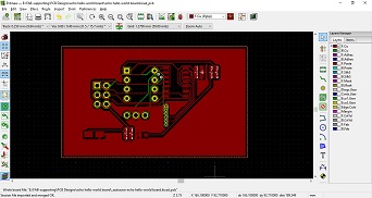
My PCB was visible like as shown in the image below:-
The white line visible in the design further has to be connected using wires till the white lines are nil. After completion of all the process the PCB would be ready to print with cuts and traces as shown in the image below:-
Now my Echo HELLO-WORLD PCB is ready to be printed in the milling machine.